
ADC In An FPGA, Part 1
Note: I first published on May 1st, 2011 in a long abandoned blog. I have republished it here, with minor edits, because it is still very relevant and useful.
I’ve always had this crazy idea to implement an ADC (Analog to Digital Converter) in an FPGA. Recently I worked out a lot of the details, enough where I started to get concerned about future patent violations and associated legal issues. I’ve decided to post a summary of my work, as a record of prior art, just in case something actually comes from this. Along the way, some other geeks might be interested in this.
This ADC is supposed to be inexpensive– that’s the main goal. My requirements for this were to have no active external components. The idea is that if you already have an FPGA with some unused pins, and add some passive components then you could have a simple ADC for almost nothing. Along that line of thought, the logic inside the FPGA should also be super small.
These design parameters makes things quite difficult, and requires some out-of-the-box thinking. Normally one would consider the traditional ADC architectures and then shoehorn that into an FPGA. But after looking at them, I decided that none of them really fit the FPGA implementation very well. So instead of doing a top-down approach, I went with the bottom up.
At the core, all ADC’s rely on some sort of voltage comparator. In the FPGA, the only real comparator would be a differential input buffer. LVDS, for example. Of course, such a buffer has lots of bad behaviors like hysteresis– but that’s all we have to work with. The architecture I came up with should work around these issues.
Below is a block diagram for my ADC, click on it to enlarge. For the moment, ignore the RC Filter Model and Low Pass Filter.
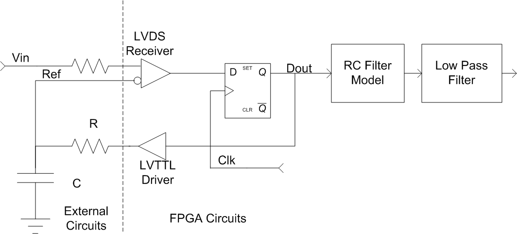
Normally, Ref would mostly track Vin. The LVDS receiver, used as a voltage comparator, senses if Ref is too high or too low, and feeds the external RC filter accordingly. There will be some ripple on Ref, which is mostly the result of the RC filter characteristics and the hysteresis of the LVDS receiver. Oddly enough, however, this ripple helps the circuit.
The RC Filter Model is simply a digital representation of the external RC filter. The output of this block is the voltage of the Ref signal (including all the ripple). The Low Pass Filter is there to smooth out the ripple on the RC Filter Model.
That’s it! OK, the devil is in the details, but that’s most of it. I’ll get to some of those details, but let’s look at some waveforms.
For these waveforms and unless otherwise said, Vin is a 10 KHz sine wave from 0.4v to 2.9v, C=220 pF, R=3.3K ohms, and the LVDS receiver hysteresis is 50 mV.
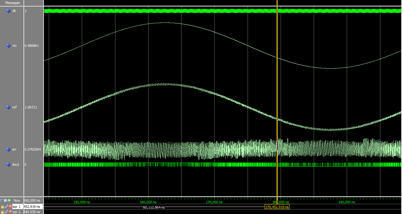
In the image above, you’ll see Vin doing it’s thing with Ref tracking it. Of course Ref has the expected ripple. The Err signal is the difference between Vin and Ref, and has a swing of about +/- 65 mV. Dout and Clk are there, but when zoomed out this far you can’t see anything useful. Here is the same waveforms, but zoomed in a lot:
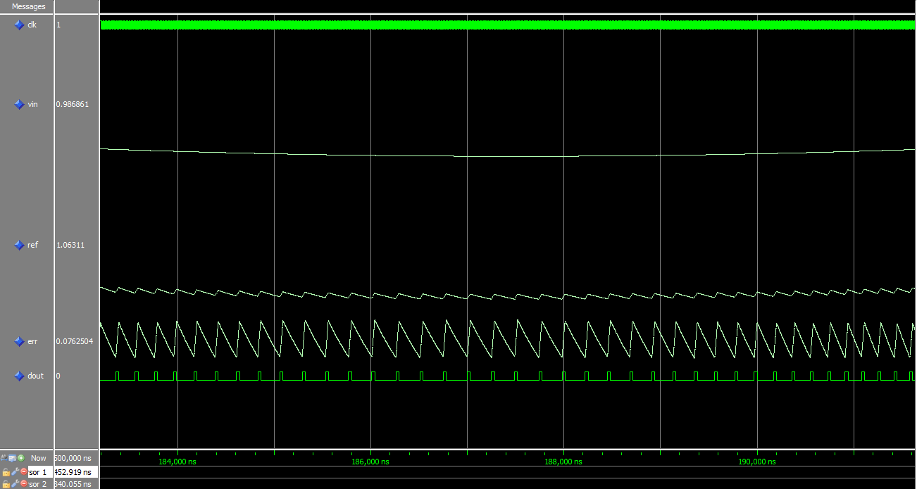
In this image you can clearly see the ripple, and resulting Err, on Ref. You can also see Dout. One thing that should be mentioned at this point is that Dout is not simply a PWM’d representation of Ref. As Ref changes voltage, the ability for Dout to charge/discharge the external cap changes due to the voltage across R. This image shows Ref when it’s at its lowest level, so Dout has an easy time driving Ref higher but has difficulty bringing it lower. This is shown as a change in slew rate on Err, fast rising edge and slow falling edge.
The LVDS hysteresis and RC time constant will effect the ripple frequency. Also, this frequency will slow down as Vin/Ref get closer to the power and ground rails. As a general rule, you want this ripple to be as high frequency as possible while still maintaining a somewhat analog appearance. I’ve found that 220 pF and 3.3K Ohms is about the shortest RC time constant that’s practical using LVDS and LVTTL.
The RC Filter Model sounds daunting at first, but isn’t too bad in reality. First, we’ll go over the math. The formula is this:
Ref_New= Ref_Current + (Dout-Ref_Current) * (1-exp(-T/RC))
Where Ref_New is the new value of Ref, Ref_Current is the current value of Ref, Dout is either 0.0 or 3.3 depending on the state of Dout, T is the clock period in seconds, R is in ohms, and C is in farads. The function exp(x) returns e to the power of x.
In the FPGA, it’s only the last part of that formula that’s hard, the “* (1-exp(-T/RC))” part. But on closer inspection it’s not that bad. Since T, R, & C do not change at runtime, the whole thing becomes a multiplication by a constant. That’s a good thing, because doing an exp() function in an FPGA is challenging and uses lots of logic.
That constant would normally be represented as fixed point. By careful selection of R and C, that constant can have very few ‘1’ bits in it– maybe even a single ‘1’ bit. This is super important. Fixed point multiplication by a number with a single ‘1’ bit is the same as a bit-shift! And, as you know, a bit-shift in an FPGA takes no logic. If there are two ‘1’ bits then it’s two shifts and an addition– still not bad. One of my goals in the near future is to write a program that will find combinations of T, R, and C that make the math easier. I’ve done something similar in the past and it works out really slick.
Another “optimization” is to scale the numbers. Instead of Ref being represented by a fixed point number from 0.0 to 3.3, it can be represented as 0.0 to 0.999999. In binary, that would be from “00000000” to “11111111”. While that doesn’t make the math any easier, it does make the ADC somewhat independent of the I/O Standards used, and puts the ADC output in a more useful form.
The Low Pass Filter can be just about anything, depending on what quality of output you require. A simple averaging filter can be good enough for most things. For better performance, there are many types of IIR filters that would work well. I don’t recommend a FIR filter for this, due to the sample rates and the number of taps that you would need.
It’s a little preliminary to talk about performance of this ADC. I have simulated enough of this to know that the theory is sound, but I have not built an actual circuit or done an FFT analysis on the output. But based on what I’ve seen so far, it seems like a slam dunk to get 10 KHz bandwidth (20 KHz output sample rate) and 12-bit performance. Higher sample rates are possible with sacrificing rail to rail operation and bit resolution.
I should also mention that the same RC Filter Model can be used to make a nice DAC in an FPGA. Doing so would be better than using PWM or a first-order Delta Sigma modulator (similar to a Xilinx app note) in that the DAC settling time is faster, it has a more linear input to output response, and can operate with a faster RC time constant resulting in better frequency response.